High Speed Imaging Interface
A high speed imaging interface platform designed to integrate a 29.8MP image sensor with controlled LVDS data paths, precision power delivery, and thermal optimized architecture for reliable operation under high data throughput.
Year
01.26
Scope
High Speed Digital Design, Signal Integrity
Timeline
7 weeks
High bandwidth imaging interface with controlled LVDS routing and thermal optimized design
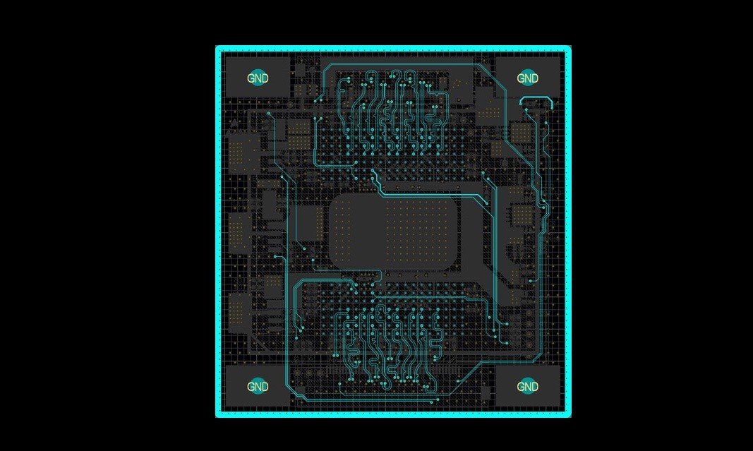
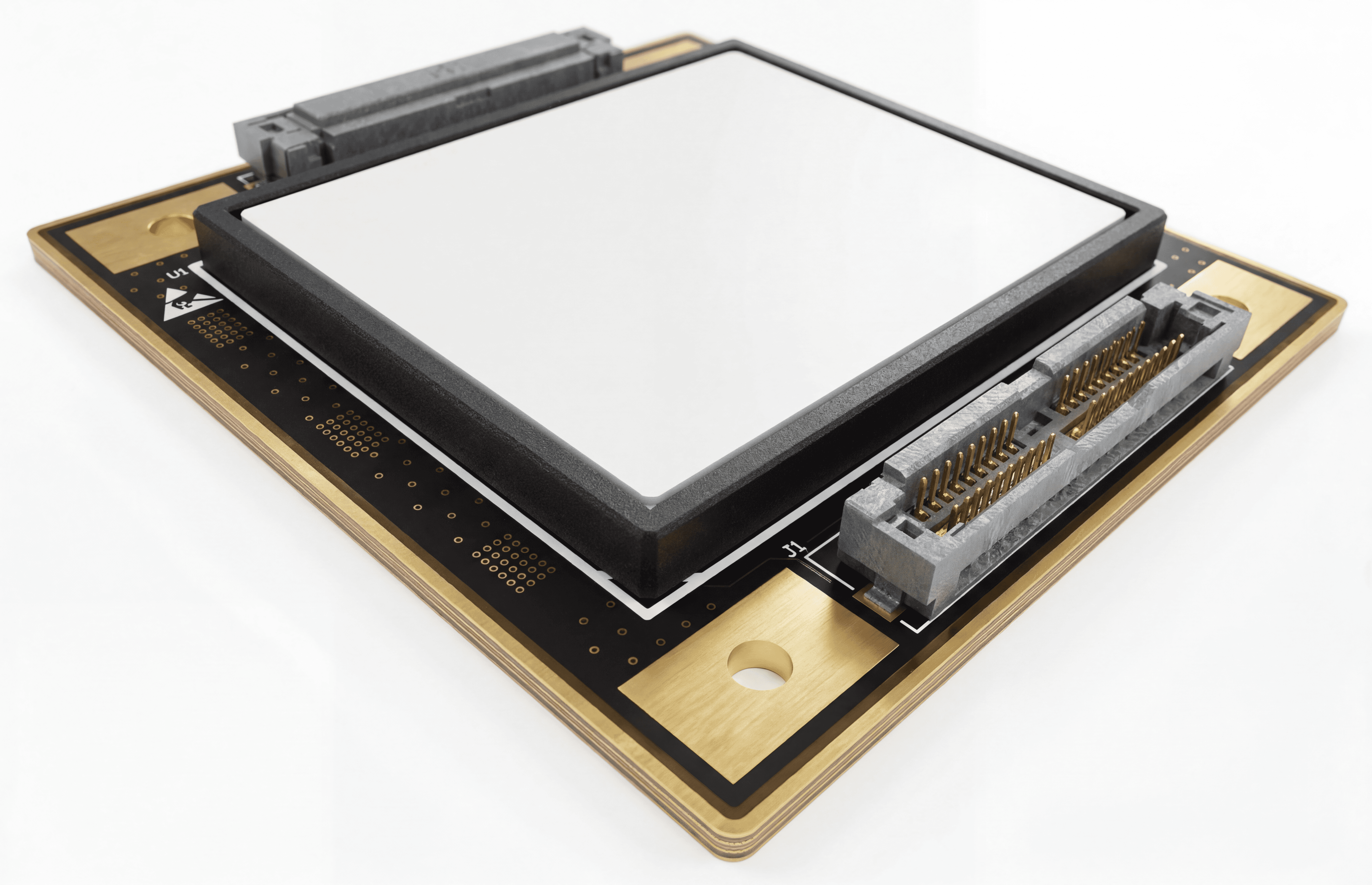
This project involved the development of a high speed imaging interface platform for a 29.8MP image sensor, with a strong focus on signal integrity, power stability, and thermal performance. The design centers around a high density sensor interface with fine pitch BGA escape and controlled fanout strategy. High speed LVDS data paths were carefully routed with impedance control and length matching to ensure reliable transmission and minimal skew across all lanes. All high speed signals are routed to a flexible printed cable interface, enabling integration into external processing systems while maintaining signal integrity across the PCB to FPC transition. Thermal management was a critical aspect of the design. The sensor and surrounding circuitry were supported with dedicated thermal paths, including copper distribution and via structures to efficiently dissipate heat. Layout strategy was optimized to balance thermal spreading with high speed signal routing, ensuring stable operation under sustained load conditions. Power architecture was designed for noise sensitive imaging operation, with dedicated regulation and filtering to provide clean supply rails. Sensitive analog domains were carefully isolated from high speed digital paths to reduce coupling and preserve signal quality. The result is a compact and robust imaging interface platform capable of supporting high resolution data acquisition with stable thermal behavior and reliable high speed signal transmission.